This article is produced and financed by NTNU Norwegian University of Science and Technology - read more
The future’s fastest tech gadgets may get Norwegian help
Researchers in Norway may be on the cusp of a solution to make tech gadgets even smaller and more powerful.
Our tech gadgets are getting ever smaller and require ever greater capacity. This demands that their components make better use of the shrinking space.

The parts can be produced using a technique called nanolithography. Nanolithography uses light to draw patterns on a tiny scale, but this is no longer good enough.
“We think we can do this with atoms instead of light,” says Ingve Simonsen, a professor at NTNU’s Department of Physics.
He is part of Nanolace, a new project that aims to contribute to even more efficient tech gadgets. Nanolace is headed by Professor Bodil Holst from the University of Bergen. Several NTNU researchers and five European partners are also participating.
The EU is so confident in what the project partners are doing that Nanolace is being supported by the EU programme FET Open. This programme gives people who have possible solutions for future technologies a chance to test their theories in practice.
Controlling the light
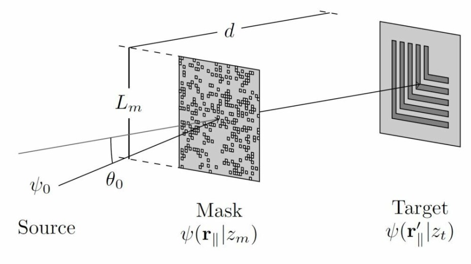
Today, a common method of making tiny data components is to send light through a mask, which is a kind of filter. By adjusting the mask, you can shape the light beam that has passed through the mask to form a pattern on the other side of it.
If the filtered light hits a surface that responds to light, you can draw a pattern onto that surface. That is how you create the miniscule patterns required to make complicated circuit boards and microchips.
But the technique has its limitations.
Not precise enough
We have a problem when the structures in the pattern we want to create become comparable to the wavelength of the light. Then the patterns we produce with nanolithography are blurry – and therefore useless.

Traditionally, we’ve solved this problem by reducing the wavelength of the light source. But when we do that, the energy of the light particles – the photons – increases.
Now we’ve reached a crossroads where we can’t increase the photon energy anymore. If we do, the light particles build up enough energy to kick the electrons in the materials we’re using up to higher energy levels. In other words, the light ionizes the material.
Photons are emitted when these electrons drop back down to their normal, lower energy levels. Unfortunately, the photons fly in all directions, even where they shouldn’t be, which means we can’t create the pattern we want.
The minimum achievable size for patterns is currently just over 10 nanometres wide. A nanometre is a billionth of a metre, and you might think that 10 nanometres would be small enough, but that doesn’t always cut it.
Advantages of atoms
That brings us to the need for a new method to create even more minute structures. By using neutral and metastable atoms instead of light, all the nonsense with energy levels and imprecise patterns can be avoided.
“We believe we can create patterns as small as one nanometre wide,” says Simonsen.

The technique works. In theory.
“Technically, it’s possible at least,” says Simonsen.
Torstein Nesse recently received his PhD at NTNU, where he wrote two articles about the technique that were part of his research work.
His articles showed that it is possible to use atoms instead of light to create even smaller nanoscale patterns – at least in computer simulations. Atoms have considerably less wavelength than light at the same energy. This method using atoms would potentially enable printing smaller structures than using light. Without Nesse’s research efforts, it is doubtful that the EU would have been interested enough to support further tests.
What materials will they use for drawing?
“We don’t yet know if the technique will work in practice,” says Simonsen.
In the upcoming experiments, researchers will use a beam of metastable helium atoms for drawing new patterns.
Part of the challenge now is finding a material to draw on.
“We’re confident we’ll figure this out,” Simonsen says.


